


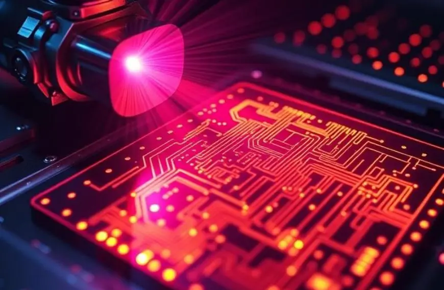
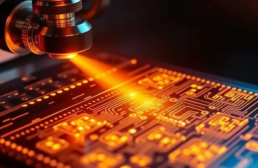
Imagine a master artist, meticulously sketching designs onto a canvas. In semiconductor fabrication, this canvas is a silicon wafer, and the artist’s tool is light. Lithography involves projecting light through a mask, a stencil of the desired circuit pattern, onto a photosensitive layer atop the wafer. This process engraves the intricate pathways that allow electrons to dance through microchips, powering our devices.
The wavelength challenge: pushing the boundaries
Traditionally, Deep Ultraviolet (DUV) lithography, using light with a 193-nanometer wavelength, was the industry standard. However, as the demand for smaller, more powerful chips grew, DUV reached its physical limits. It’s akin to trying to draw finer lines with a broad-tipped pen; there’s only so much detail you can achieve.
Enter EUV Lithography: A quantum leap
To overcome these limitations, scientists turned to EUV lithography, which employs light at a dramatically shorter wavelength of 13.5 nanometers, nearly 14 times shorter than DUV. This shift is like swapping that broad-tipped pen for an ultra-fine quill, enabling the drawing of incredibly detailed patterns.

The Alchemy of EUV: Conjuring light from plasma
Generating EUV light is no small feat. It involves firing high-powered lasers at tiny droplets of tin, creating a plasma that emits the coveted 13.5-nanometer wavelength. This process occurs within a vacuum chamber to prevent the absorption of EUV light by air molecules. The emitted light is then focused and directed onto the silicon wafer using a series of sophisticated mirrors, as traditional lenses would absorb EUV light.
Challenges on the EUV frontier
While EUV lithography is a technological marvel, it comes with its own set of challenges. The complexity of generating and handling EUV light makes the equipment extraordinarily expensive and intricate. Moreover, the process requires a pristine environment, as even the slightest contamination can disrupt the delicate patterns being etched.
The Impact: Powering the future
Despite these hurdles, EUV lithography has revolutionized chip manufacturing, enabling the production of microchips with features as small as 7 nanometers and paving the way for even smaller nodes. This advancement translates to more powerful, energy-efficient, and compact electronic devices, fueling innovations from smartphones to supercomputers.
The ongoing journey
The evolution from traditional lithography to EUV represents a monumental leap in our ability to miniaturize and enhance electronic components. As researchers continue to refine EUV technology and explore beyond, the horizon promises even more astonishing advancements in the world of semiconductors.
Note: This narrative is based on information available up to February 2025.


